Content for TS 37.461 Word version: 17.1.0
4.3 Modem option
4.3.1 Interference with existing systems
4.3.1.1 Carrier frequency and frequency stability
4.3.1.2 Modem isolation and modem emissions
4.3.1.3 Modem intermodulation attenuation
4.3.2 Recovery time
4.3.3 Impedance
4.3.4 Modulator characteristics
4.3.4.1 Levels
4.3.4.2 Spectrum emission mask
4.3.5 Demodulator characteristics
4.3.6 Duty cycle variation
4.3.7 Operating bands
4.3.8 Time delay and accuracy
4.3.9 Insertion Loss
4.3.10 DC port isolation
4.3.11 RET control unit spurious emission
4.3.12 Control unit spurious emission
4.3 Modem option p. 7
The connection to a RET and/or a TMA control unit by way of a coaxial cable which is shared with DC supply and RF signals is provided by two modems, a BS modem and an antenna modem. The BS modem shall be either connected to the antenna connector of the BS or integrated in the BS. It provides signal transmission to the antenna modem and signal reception from the antenna modem over the antenna feeder cable. The antenna modem is located between the antenna feeder cable and the antenna. Modem configurations and reference points for modem characteristics are specified in Figure 4.3.1 and Figure 4.3.2. Unless otherwise stated, requirements in this section apply to both BS modem and antenna modem.
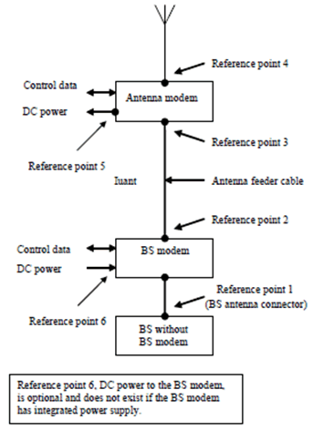
Figure 4.3.1: Modem configuration and modem reference points for a BS without BS modem
(⇒ copy of original 3GPP image)
(⇒ copy of original 3GPP image)
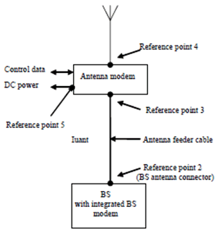
a BS with integrated BS modem
4.3.1 Interference with existing systems p. 9
The modem circuit shall be capable of managing its transmitting characteristic according to subclause 4.3.5.
4.3.1.1 Carrier frequency and frequency stability p. 9
The following carrier frequency shall be used for this application:
2.176 MHz ± 100 ppm
4.3.1.2 Modem isolation and modem emissions p. 9
The external BS modem shall provide minimum attenuation according to Figure 4.3.1.2.1 between reference point 2 and reference point 1 to protect the BS from emissions of the antenna modem.
External BS modem emissions at reference point 1 shall be attenuated at least according to the modem attenuation in Figure 4.3.1.2.1 below the levels specified for the modem spectrum emission mask in subclause 4.3.4.2 to protect the BS from emissions of the BS modem.
The antenna modem shall provide minimum attenuation according to Figure 4.3.1.2.1 between reference point 3 and reference point 4 to protect other radio systems from emission of the BS modem.
Antenna modem emissions at reference point 4 shall be attenuated at least according to the modem attenuation in Figure 4.3.1.2.1 below the levels specified for the modem spectrum emission mask in subclause 4.3.4.2 to protect other radio systems from emission of the antenna modem.
4.3.1.3 Modem intermodulation attenuation p. 10
The modem intermodulation attenuation is specified in terms of the power in intermodulation products of WCDMA modulated carriers present at reference point 1 or reference point 3.
For 2 downlink carriers of 43 dBm the power of third order intermodulation products in the UL operating bands for the external BS modem and antenna modem shall not exceed:
- - 130 dBm/100 kHz for frequencies < 1 GHz
- - 120 dBm/1 MHz for frequencies ≥ 1 GHz
- - 98dBm/100kHz
- - 135 dBm/100 kHz for frequencies < 1 GHz
- - 125 dBm/1 MHz for frequencies ≥ 1 GHz
4.3.2 Recovery time p. 10
A minimum recovery time shall be allowed between receiving and transmitting messages on the bus. For this reason a minimum permitted response time is specified in subclause 4.5 in TS 37.462.
4.3.3 Impedance p. 10
The modem transceiver shall provide constant impedance in both transmitting and receiving modes:
- Nominal impedance Z0: 50 Ω;
- Return loss at modem carrier frequency ± 0.1 MHz > 10 dB;
- Return loss in external BS and antenna modem operating bands > 20 dB.
4.3.4 Modulator characteristics p. 11
4.3.4.1 Levels p. 11
ON-Level:
+3 dBm ± 2 dB
OFF-Level:
≤ -40 dBm
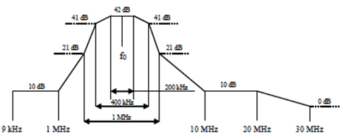
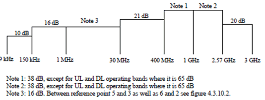
4.3.4.2 Spectrum emission mask p. 11
The modem spectrum emission mask is specified in Figure 4.3.4.2.1. Intermediate values may be obtained by linear interpolation between the points shown. The corresponding measurement bandwidths are specified in Table 4.3.4.2.1. For modem configurations according to Figure 4.3.1 the BS modem emissions shall not exceed the limits of the spectrum emission mask at reference point 2. For modem configurations according to Figure 4.3.2 the BS with integrated BS modem emissions shall not exceed the limits of the spectrum emission mask at reference point 2 only for frequencies below 20 MHz. Antenna modem emissions shall not exceed the limits of the spectrum emission mask at reference point 3.
| Band | Measurement Bandwidth |
|---|---|
| 9 kHz - 150 kHz | 1 kHz |
| 150 kHz - 30 MHz | 10 kHz |
| 30 MHz - 1 GHz | 100 kHz |
| 1 GHz - 12.75 GHz | 1 MHz |
4.3.5 Demodulator characteristics p. 11
The demodulator shall fulfil the requirement in subclause 4.3.6 for a carrier ON-Level within +5 dBm to -12 dBm and a carrier OFF-Level less than -18 dBm. The levels within -12 dBm to -18 dBm are undefined.
4.3.6 Duty cycle variation p. 11
In order to guarantee proper transmission of data bits through the processes of modulation and demodulation, the following limit shall be met for the duty cycle variation:
ΔDCSYSTEM = |DCRX - DCTX| ≤ 10 %
Where: ΔDCSYSTEM is the difference between the duty cycles of the transmitted and received bit streams,
DCTX = Duty cycle for the input bit stream, and
DCRX = Duty cycle for the output bit stream.
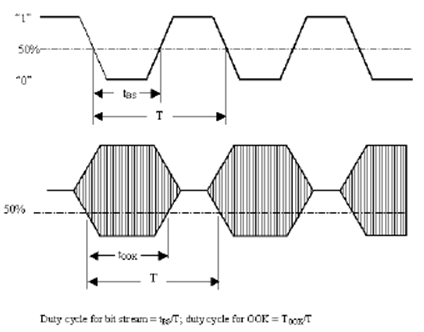
Figure 4.3.6.1: Duty cycles of the bit stream and OOK modulated subcarrier
(⇒ copy of original 3GPP image)
(⇒ copy of original 3GPP image)
For transmission through a coaxial cable, two converters are required, one from a bit stream to OOK (modulator) and one from OOK back to a bit stream (demodulator). Therefore half of the total duty cycle tolerance is available for each converter.
For an input bit stream with a duty ratio of 50 %, the cascaded modulator and demodulator shall provide an output bit stream with a duty ratio within the limits 40 % - 60 %, measured in each case at 0.5 times peak amplitude (see Figure 4.3.6.1).
4.3.7 Operating bands p. 12
A UTRA/FDD BS, UTRA/TDD BS, E-UTRA BS, NR BS or antenna modem is designed to operate in one or several of the operating bands defined in TS 25.101, TS 36.101 and TS 38.101-1.
The operating bands of the BS modem or antenna modem shall be declared by the manufacturer.
4.3.8 Time delay and accuracy p. 12
The time delay in the operating bands shall be declared by the manufacturer with ± 1 ns accuracy. The time delay shall not exceed 30 ns. This requirement is only applicable to external BS modem and antenna modem.
4.3.9 Insertion Loss p. 12
The insertion loss in the external BS modem or antenna modem operating band shall be ≤ 0.3 dB.
The actual insertion loss shall be declared by the manufacturer.
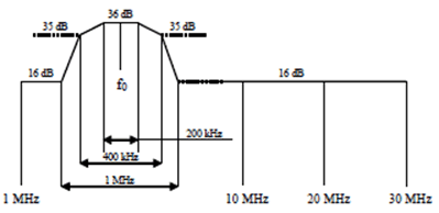
4.3.10 DC port isolation p. 13
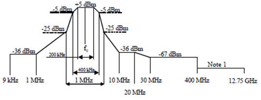
The isolation between DC port and RF ports shall meet the minimum values in Figure 4.3.10.1 and Figure 4.3.10.2. Figure 4.3.10.1 is valid for antenna modems between reference point 5 and 4 as well as 5 and 3 and for BS modems without integrated power supply between reference point 6 and 2 as well as 6 and 1. Figure 4.3.10.2 is valid as additional requirement for antenna modems between reference point 5 and 3 and for BS modems without integrated power supply between reference point 6 and 2.
4.3.11 RET control unit spurious emission p. 13
Void.
4.3.12 Control unit spurious emission p. 13
The control unit, or a combination of control units, shall not generate spurious emission, at reference point 5, above a level that will violate the spectrum emission mask requirement according to clause 4.3.4.2. The DC port isolation according to clause 4.3.10 shall be taken into account.
![]()
![]()
![]()